
Anderon — an IBM Company
America’s first pure-play quantum foundry — an IBM-capitalized spinout headquartered in Albany, New York
Anderon LLC is not an independent, venture-backed startup — it is a standalone subsidiary capitalized by IBM (NYSE: IBM) with cash, intellectual property, and personnel. Its formation was announced via a Letter of Intent between IBM and the U.S. Department of Commerce on May 21, 2026, and operations formally commenced with the execution of a definitive CHIPS Act award agreement on September 16, 2026. The company is headquartered in Albany, New York, and was built atop IBM’s more than two decades of semiconductor R&D infrastructure at the Albany NanoTech Complex — a structural distinction that gives Anderon a materially different risk and governance profile than a typical early-stage startup.
Holds an M.S., M.Phil., and Ph.D. in Electrical Engineering from Yale University (B.E. from Bombay University, M.Tech. from IIT Bombay). Joined IBM in 1998 and went on to lead IBM’s Semiconductors Division as General Manager while serving as Vice President of Hybrid Cloud research at IBM Research, driving 7nm, nanosheet, and 2nm process development. Led formation of the $2.3B AI Hardware Center in 2019 and the $10B High-NA EUV research center at Albany NanoTech in 2023. Chairs the board of the Semiconductor Research Corporation (SRC) and was named Asian American Executive of the Year in 2021.
Leads IBM’s quantum computing roadmap, including the Heron and Nighthawk processor families and the company’s 2033 target for a large-scale fault-tolerant system, “Starling.” He is driving the manufacturing-transition strategy through the Anderon partnership and has publicly stated that the shift from 200mm to 300mm wafers multiplies device complexity tenfold and triples per-line output, accelerating overall throughput roughly 30-fold.
Told Reuters that Anderon will position IBM’s chipmaking capabilities for external customers on the same terms IBM uses internally, and said the company is already in discussions with potential clients. No specific customer names or contract sizes have been disclosed.
Led the announcement of the CHIPS Act quantum package totaling $2.013 billion across nine companies, stating the “strategic quantum technology investments will build on our domestic industry, creating thousands of high-paying American jobs.” The Commerce Department attached a minority, non-controlling equity stake condition to all nine recipients.
Anderon’s board composition, equity allocation, and the minority-stake percentage held by the government or any other investor relative to IBM are not disclosed. IBM has referenced the possibility of “additional investors” joining as the company grows, but no confirmed outside investor has been named to date. Per available reporting, IBM effectively retains full ownership and control, which warrants a governance-transparency assessment distinct from that applied to independent deep-tech startups.
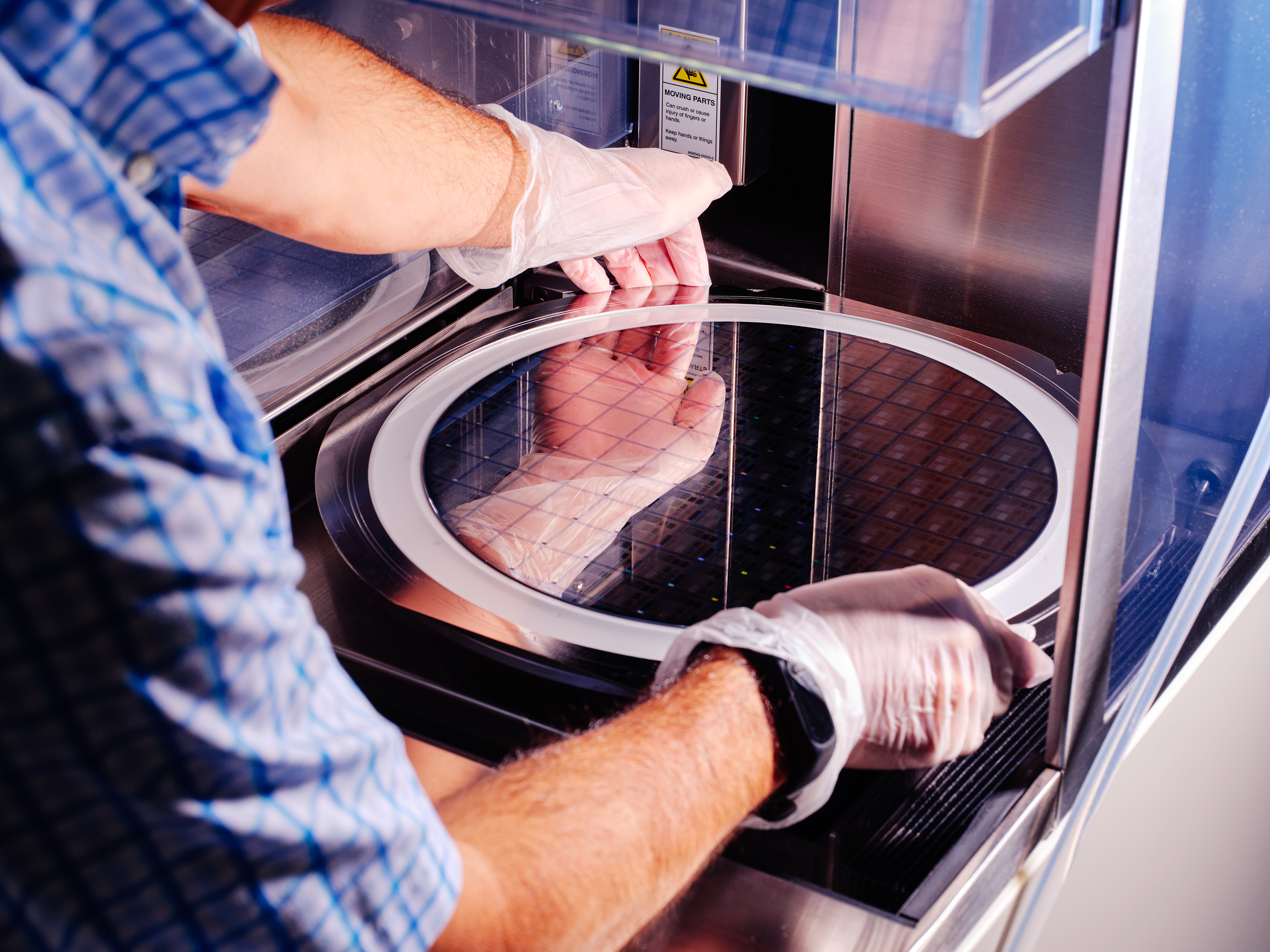
Anderon operates a 300-millimeter pure-play quantum foundry in Albany, New York, and per company disclosure has already begun running its first quantum wafers through the manufacturing line. We view this as a credible early operating milestone demonstrating the ability to translate pre-production research into commercial-grade output — while flagging that no quantitative disclosure of external customer revenue or order backlog has yet been made.
Anderon’s business model appears to rest on three distinct demand pillars.
Manufactures specialized wafers supporting high-performance superconducting qubit arrays, quantum I/O signaling, and readout signal-chain components, sold as foundry services to customers across the quantum ecosystem. The company has stated plans to expand beyond superconducting modalities over time.
IBM’s own quantum processor roadmap (Heron r2, Nighthawk, and beyond) and its 2033 target for a large-scale fault-tolerant system, “Starling,” provide an internal volume anchor for early capacity utilization. In June 2026, IBM separately announced a commitment to invest more than $10 billion in quantum computing over the next five years across R&D, capex, ecosystem partnerships, and M&A.
Current production is concentrated on superconducting-qubit wafers, but the company has publicly stated intent to expand foundry services into other quantum modalities (e.g., trapped-ion, neutral-atom). No specific timeline or investment scale has been disclosed.
The Albany NanoTech Ecosystem: Located on the SUNY Polytechnic campus, the Albany NanoTech Complex has attracted more than $20 billion in cumulative public-private investment and is the largest such semiconductor R&D facility in the country, co-located with tenants including GlobalFoundries, Samsung, and Applied Materials. IBM has conducted semiconductor research there for over two decades, delivering milestones such as nanosheet transistor technology and the world’s first demonstrated 2nm node. Because Anderon scales an existing operating platform rather than building from scratch, we view its time-to-production as structurally faster than a newly formed foundry would achieve.
We believe the near-term addressable external customer base is likely to be limited. Per industry reporting (Tom’s Hardware, among others), the pool of potential superconducting-qubit customers is confined to a small set of companies — Rigetti, IQM, SEEQC, and a handful of others — and whether any of them will actually route wafer production through a facility owned by their largest competitor remains an open question flagged by multiple industry analysts. No quantitative disclosure of signed external customer contracts, order backlog, or revenue visibility is available as of this writing.
Anderon’s capitalization does not follow a conventional VC round structure; instead, it combines direct parent-company funding from IBM with an industrial-policy grant under the CHIPS and Science Act. The pivotal event is the September 16, 2026 execution of a definitive CHIPS Act R&D award agreement, which converted the non-binding May 2026 Letter of Intent into a binding commitment.
IBM and the U.S. Department of Commerce signed a Letter of Intent proposing a $1 billion CHIPS Act R&D incentive, formalizing plans to form the new subsidiary Anderon. IBM simultaneously announced a matching $1 billion cash contribution plus intellectual property, assets, and skilled workforce, and flagged the possibility of additional future investors. The same day, Commerce announced a broader $2.013 billion CHIPS quantum package spanning nine companies, including $375 million for GlobalFoundries.
IBM disclosed a plan to invest more than $10 billion in quantum computing over the following five years, spanning R&D, capital expenditure, ecosystem partnerships, and M&A — reported as the largest single-company quantum computing commitment disclosed to date, and a signal of the parent-level capital support underpinning Anderon’s medium-term capitalization.
Deal structure: The $1 billion CHIPS Act R&D award proposed under the May LOI was converted into a binding agreement between the U.S. Department of Commerce and Anderon (an IBM company). Combined with IBM’s matching $1 billion cash contribution, total capital deployed into Anderon reaches $2 billion.
Strategic significance: Anderon CEO Mukesh Khare said the agreement “strengthens our ability to deliver the manufacturing scale the quantum industry needs,” while IBM Research Director Jay Gambetta stated that “Anderon’s focus on wafer fabrication … strengthens our ability to execute and accelerate progress toward the next era of quantum computing.”
Market-confidence signal: In our assessment, the federal government’s execution of a binding $1 billion R&D award to a spinout entity less than four months old reflects a high degree of policy conviction in the superconducting-qubit modality and in IBM’s manufacturing execution. At the same time, we note this exposes the company’s capital structure to industrial-policy and administration-change risk.
• Total capitalization: $2,000,000,000 ($1B CHIPS Act award + $1B IBM cash contribution)
• Government equity condition: Commerce attached a minority, non-controlling equity stake condition to all nine CHIPS quantum package recipients, but Anderon’s specific stake percentage was not disclosed in the September 16 announcement
• Comparable benchmark (1): Within the same package, GlobalFoundries disclosed a separate agreement granting Commerce a 1% equity stake
• Comparable benchmark (2): In the August 2025 Intel CHIPS conversion, the administration took an approximately 10% equity stake (valued at roughly $8.9 billion at the time) — suggesting Commerce is applying a consistent framework across recipients
• Package weighting: Anderon’s $1 billion award represents roughly half of the total $2.013 billion nine-company package, and is approximately 50x the size of the smallest recipient, Diraq ($38 million)
• Milestones/conditions: No specific technical or financial milestones tied to the award were disclosed in the September 16 announcement
Anderon’s competitive position rests on (1) the largest wafer format in the industry (300mm), (2) more than two decades of accumulated Albany NanoTech infrastructure, and (3) a dual anchor-capital structure spanning the federal government and its parent company. We note, however, that a significant share of these advantages is structurally tied to dependence on IBM, which cuts against Anderon’s credibility as a genuinely independent foundry — a tension we flag explicitly below.
Per IBM Research Director Jay Gambetta, the shift from 200mm to 300mm multiplies device complexity tenfold and triples per-line output, accelerating overall throughput roughly 30-fold. Competing quantum foundries such as SkyWater Technology remain on 200mm processes, making Anderon the only quantum-dedicated foundry operating at 300mm production scale, per available reporting.
Because Anderon scales an existing operating platform rather than building from scratch, its time-to-production is structurally faster than a newly formed foundry’s would be. The company has already achieved the operational milestone of running its first quantum wafers through the manufacturing line, consistent with two-plus decades of accumulated equipment, workforce, and process know-how that cannot be replicated quickly.
Receiving the largest single allocation ($1B, roughly half) within the $2.013 billion CHIPS quantum package signals a high degree of federal conviction in the superconducting-qubit modality. At the same time, this concentrates the company’s capital structure exposure to industrial-policy and administration-change risk — a factor we weigh as both a strength and a risk, not as a strength alone.
Unlike independent quantum foundries that must secure early utilization from scratch, Anderon can draw on IBM’s own quantum processor cadence and its 2033 Starling target as anchor demand. Paradoxically, this same relationship is what raises the market’s central open question: whether competing quantum hardware companies have genuine incentive to route production through a facility owned by their largest rival.
Overall assessment: Anderon’s leadership is not a conventional VC-backed founding team but an “internal spinout” management structure — a career IBM semiconductor and quantum R&D executive (Mukesh Khare) as CEO, paired with IBM’s own quantum roadmap lead (Jay Gambetta) — which structurally distinguishes it from typical early-stage deep-tech startups. This is a strength from a scientific and operational execution standpoint, but in our view the company’s governance independence and its capital and decision-making dependence on parent company IBM should be weighed as a distinct risk factor by investors.